
Micron Targets 42 Gb/mm2 Density for G11 NAND in 2027
The memory maker will ramp production in late 2027, using wafer bonding to double storage density and boost I/O speeds.
By Chioma Kuznetsov ·
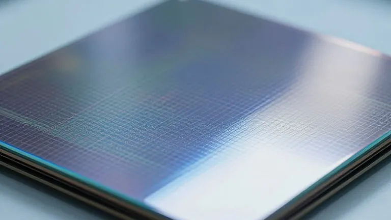
Micron Technology announced on Thursday that its next generation of 3D NAND flash, designated G11, will enter volume production in the second half of 2027. The company stated at a recent industry event that the new chips will double storage density compared to its current lineup while improving speed and energy efficiency.
The G11 architecture moves from 21 Gb/mm2 to 42 Gb/mm2 in triple-level-cell configuration. Input/output performance will increase by up to 50%, rising from 3,600 MT/s to 5,400 MT/s. Power consumption per bit will drop by more than 25%, a reduction Micron says is essential for artificial intelligence workloads that require high bandwidth and low energy use.
A key manufacturing shift underpins these improvements: wafer-on-wafer bonding. This process allows Micron to fabricate the memory array and peripheral circuitry on separate wafers before joining them. Scott DeBoer, Micron’s president and chief technology and products officer, confirmed the company is adopting this method to optimize each component independently. DeBoer called G11 the world’s most advanced NAND and said the timing for bonding is now right because it has become cost-effective.
While Micron has not disclosed the exact layer count, the G11 design will exceed 400 layers. The company attributed the density jump to a combination of additional layers and a smaller memory cell pitch. This approach distinguishes G11 from the upcoming BiCS10 product from Kioxia and the V10 product from Samsung, which Micron expects to trail in density.
Micron plans to share further technical specifications in 2027 as it prepares for high-volume manufacturing. The company said it will continue scaling in all three dimensions beyond G11. DeBoer noted that future generations will rely on high-mobility materials and ultra-dense cell architectures to reduce energy usage. The company has not yet published detailed roadmaps for products following G11.
Demand for NAND-based storage remains strong, particularly for data center and client SSD applications. Industry analysts expect the competition for higher layer counts to continue as manufacturers seek to meet growing bandwidth requirements. Micron’s move to bonding places it in direct technical competition with Chinese rival YMTC, which has already utilized the process.